Our Solutions
DSI utilizes its own proprietary version of magnetron sputtering technology known as MicroDyn®. This page lists the different types of technologies, applications, and resources available to you. We invite you to discuss your particular coating needs with our engineering staff so that we can develop a product that is best suited for your specific application, considering all aspects of optical performance, environmental factors, and cost.

Application: Aerospace and Defense - Tightly tolerances filters, durable windows, and uniformly coated AR-coated spherical, cylindrical, and domes deliver superior reliability and environmental stability. Read more »

Resources: General Capabilities Brochure - Provides information on a wide variety of highly reliable, durable, and heat-resistance optical coatings. Our exclusive technologies and custom deposition chambers offer coatings from the Visible(VIS) through the infrared longwave infrared (LWIR) spectral wavelengths. Download »
Resource: Hand Cleaning Small Coated Optics - This describes the procedure for hand cleaning of small (≤2" diameter) thin film coated optics. The steps presented are safe for most optical coatings, which are typically composed of durable dielectric and semiconductor materials. Download »
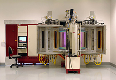
MycroDyn® Technology - MicroDyn is DSI’s proprietary version of magnetron sputtering optimized for high throughput. Read more »
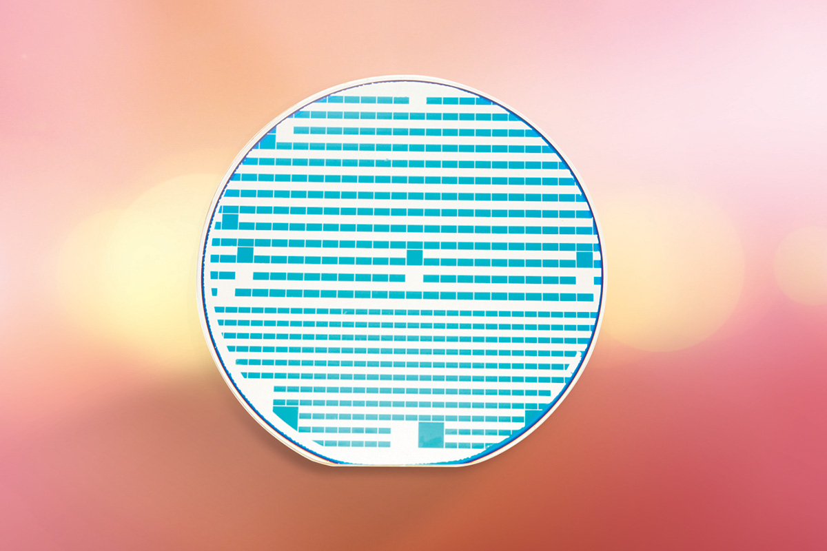
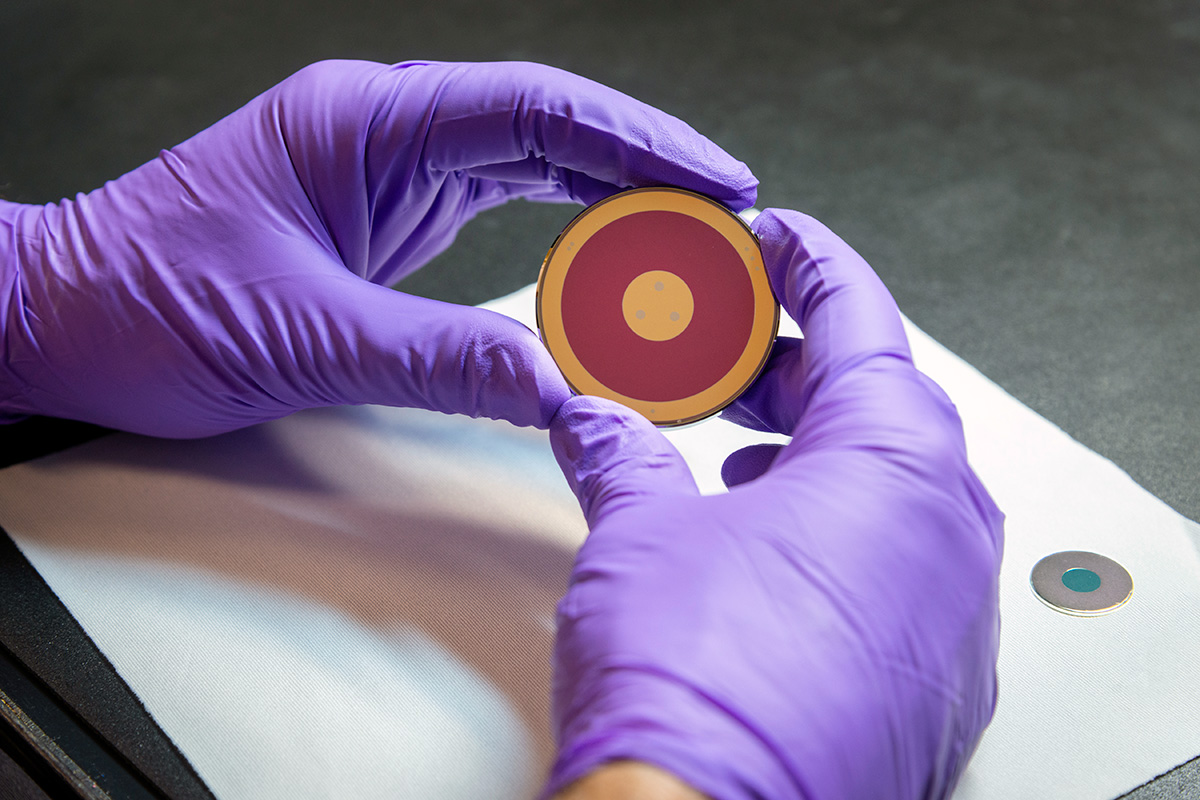
Photolithography Technology - The drive towards smaller sensors has created a need for coatings directly on semiconductor wafers. Read more »

Application: Space and Satellite - Lightweight, flexible Sunshade dielectric material protects your satellite communication devices and space components for maximum solar reflectivity, transmittance, ESD protection and thermal control. Read more »
Specifying Optical Filters for Sensor Applications - There are many subtleties that should be addressed in order to properly specify optical filters for a given application. In sensor applications, these subtleties are especially crucial in designing the best possible filter for each sensing task. Download »
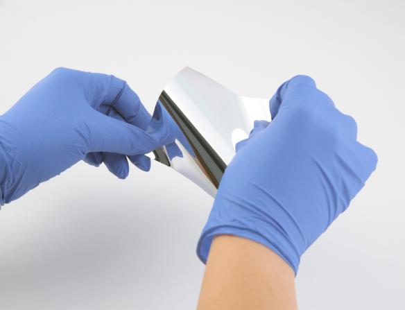
Application: A Cutting-Edge Alternative to Optical Solar Reflectors - Sunshade® Tape as a Flexible Optical Solar Rejector (FOSR) is a premier solution for spacecraft and satellite applications. Read more »

Application: AO-Resistant Material Boosts VLEO Satellite Longevity - DSI’s Sunshade® offered in both free film and tape versions. Both versions can withstand an atomic oxygen (AO) fluence greater than 1 × 10²² (AO/cm2). Read more »
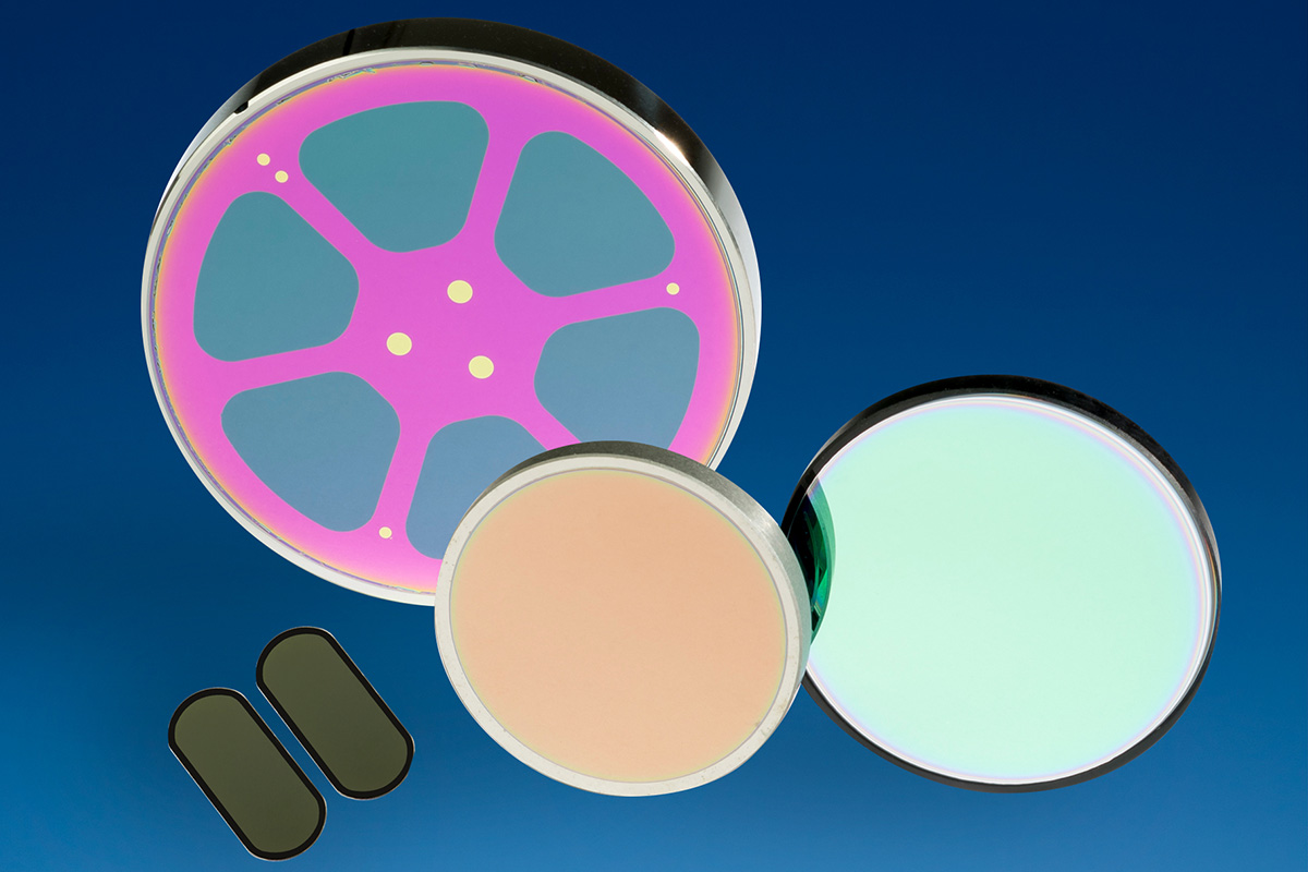
Thin Film Technology - An optical thin film consists of one or more layers of dielectric material or metal, with individual layer thicknesses. Read more »